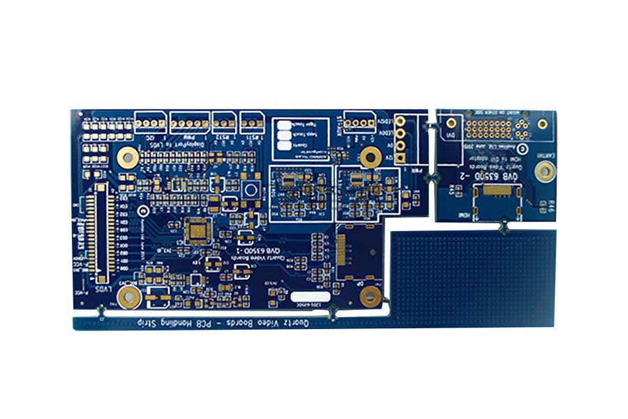
Communication Equipment PCB

Məhsul təsviri
In order to shorten the signal transmission distance and reduce the signal transmission loss, the 5G communication PCB, gradually move towards high-density wiring, fine wire spacing, the development of small aperture, thin profile and high reliability.
Communication Industry And Communication PCB
Communication Industry And Communication PCB
Communications Industry
Major Equipment
Required Communication Circuit Board
Communication PCB Features
Wi-Fi
Communication base station
Backplane, high-speed multilayer board, high-frequency microwave board, multifunctional metal substrate
Metal base, large size, high multi-layer, high frequency materials and mixed lamination
Transmission network
OTN transmission equipment, microwave transmission equipment
Backplane, high-speed multilayer board, high-frequency microwave board
High-speed material, large size, high multi-layer, high density, back drill, rigid-flex combination, high-frequency material and mixed pressure
data communication
Routers, switches, service/storage equipment
Backplane, high-speed multilayer board
High-speed material, large size, high multi-layer, high density, back drill, rigid-flex pcb
Fixed broadband
OLT, ONU and other fiber-to-the-home equipment
High-speed material, large size, high multi-layer, high density, back drill, rigid-flex PCB
Multilayer board, rigid-flex PCB
Process Difficulty Of High Frequency And High Speed PCB Board
Alignment Accuracy
Accuracy is tightened, and tolerance convergence between layers is required. The board size becomes more demanding for this convergence requirement
Size Gets Bigger
Machinability deteriorates, maneuverability deteriorates, and blind holes need to be buried 1. Cost increase 2. Difficulty in alignment accuracy
Impedance Accuracy
The etching challenge is great:
1. The etching factor: the smaller the better, the etching accuracy tolerance is 10mil and the line width is controlled by +/-1MIL, and the line width tolerance above 10mil is controlled by +/-10%.
2. Higher requirements for line width, line spacing and line thickness. 3. Others: wiring density, signal layer interference
STUB (Impedance Is Not Continuous)
STUB is tightened, board thickness fluctuation is extremely challenging, and back drilling technology is required
Increased Signal Loss Demand
It is a big challenge for all copper clad laminates; the tolerance requirements for PCB thickness are high, including length, width, thickness, perpendicularity, bow and twist, etc.
The Number Of Layers Becomes Higher
Features such as denser lines and vias, larger cell size, thinner dielectric layer, etc., more stringent requirements for inner layer space, interlayer alignment, impedance control, and reliability
Accumulated Experience In Manufacturing Communication Board Of Huihe Circuits
High Density Requirements:
The influence of crosstalk (noise) will decrease as the line width/spacing (L/S) shrinks.
Strict Impedance Requirements:
Characteristic impedance matching is the most basic requirement for high-frequency microwave boards. The greater the impedance, the greater the ability to prevent the signal from penetrating the dielectric layer, the faster the signal transmission and the smaller the loss.
Transmission Line Production Accuracy Is High:
The transmission of high-frequency signals has strict requirements on the characteristic impedance of the printed wire, that is, the production accuracy of the transmission line is generally ±lmil, and the edges of the transmission line must be very neat, and no burrs, gaps, or repairs are allowed. line.
Mechanical Processing Requirements:
First, the high-frequency microwave board material is very different from the epoxy glass cloth material of the printed board in terms of machining; secondly, the processing accuracy of the high-frequency microwave board is higher than that of the printed board. Many, the general shape tolerance is ±0.1mm (in the case of high accuracy, the shape tolerance is ±0.05mm).

