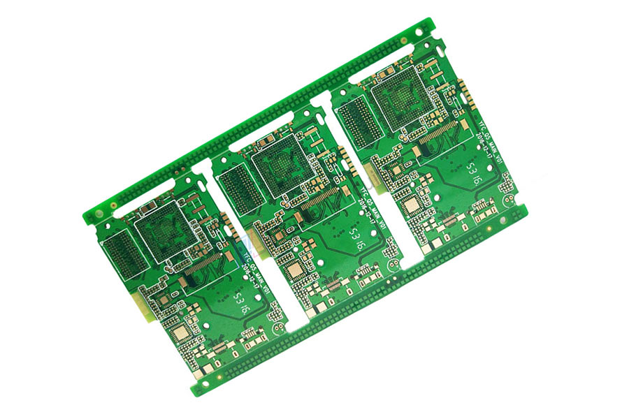
Heavy Copper PCB

Cur síos ar an Táirge
Thick copper pcb and heavy copper pcb, pcb fabrication up to 12oz, large current, pcb fabrication base material is FR4/Teflon/Ceramic, pcb fabrication used in high-power power supply and motor circuits products. HUIHE CIRCUITS Heavy Copper PCB has passed ISO9001 / ISO13485 /IATF16949 / UL /RoHS / REACH certification.
Heavy Copper PCB List
2 Layer ENIG Heavy Copper PCB Manufacturers
4 Layer ENIG Heavy Copper PCB
6 Layer ENIG Heavy Copper PCB supplier
6 Layer ENIG Heavy Copper PCB manufacturing
6 Layer ENIG Heavy Copper PCB Fabrication Service
6 Layer ENIG Heavy Copper PCB
8 Layer ENIG Heavy Copper PCB
8 Layer ENIG Impedance Control Heavy Copper PCB
2 Layer ENIG Heavy Copper PCB
The Copper Plating Process Must Achieve The Following Aspects:
1. Add a certain value according to the area value calculated by the computer and the empirical constant accumulated in the actual production to ensure the integrity of the plating layer in the hole.
2. When the circuit board is electroplated for 5 minutes, take out the substrate and observe whether the copper layer on the surface and the inner wall of the hole is intact. It is better that all the holes have a metallic luster.
3. A certain distance must be maintained between the substrate and the substrate.
4. When the thick copper plating reaches the required electroplating time, a certain amount of current must be maintained during the removal of the substrate to ensure that the surface of the substrate and the hole will not be blackened or darkened.
5. According to the mechanical processing floppy disk for trial processing, the first part pre-inspection is carried out, and all the workpieces are processed after meeting the technological requirements.
Thick Copper Plate Quality Control
1. Strictly implement the first article inspection system to ensure that the product size meets the design requirements.
2. According to the raw materials of the circuit board, reasonably select the milling process parameters.
3. When fixing the position of the circuit board, carefully clamp it so as not to damage the solder layer and solder mask on the surface of the circuit board.
4. To ensure the consistency of the substrate dimensions, the position accuracy must be strictly controlled.
5. When disassembling and assembling, pay special attention to the barrier layer of the substrate and pad paper to avoid damage to the coating layer on the surface of the pcb circuit board.
As a Chinese pcb manufacturer, we have different types of products for sale, if you have needs, please contact us.

